
Wafer Level MEMS Test

MPI Definition
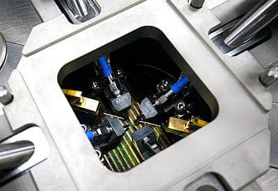
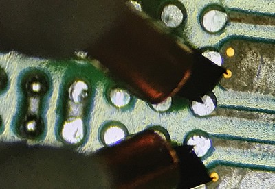
Micro Electro Mechanical Systems are chips that combine electrical and mechanical properties. These devices are used in our daily lives in a variety of ways. The constant demand for miniaturization, lightweight and cost effective solutions is driving the development of MEMS into multiple technical fields. In many cases, this technology is used for sensing a mechanical stimulus and converts it into electrical signals. The reverse transformation is done by applying an electrical signal to force a mechanical motion.
Major Requirements
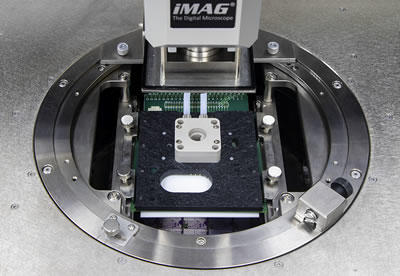
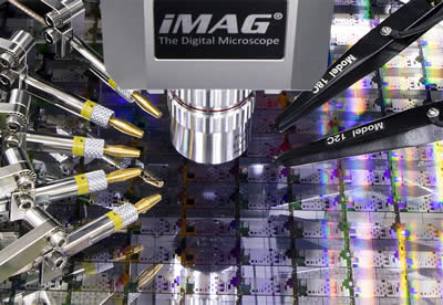
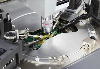
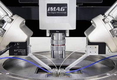
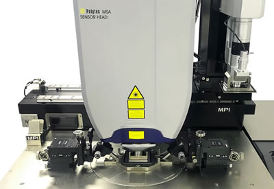
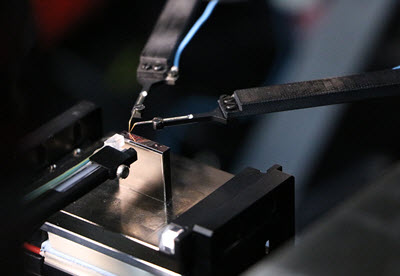
A completely stable environment is essential for testing MEMS on wafer level. Integration of additional optical measurement equipment is required to analyze the motion of the stimulated mechanical part of the MEMS. This can be dynamic in-plane and out-of-plane movements, but also very detailed topography measurements. For automated testing of entire wafers, this motion analysis system needs to work together with the alignment optics of the probe station. Testing MEMS at elevated temperatures is part of many test scenarios, but it is challenging because heat waves affecting optical measurements.
MPI Solutions
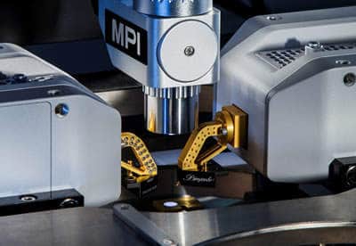
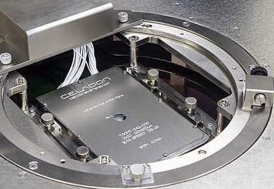
MPI probe stations are designed for highly stable on-wafer testing and feature a vibration-isolated platform that minimizes introduced ground vibrations. The TS2000-IFE has been developed specifically for this type of demanding test requirement. To design the ideal integration of optical metrology, MPI has teamed up with a major supplier of such instrumentation. The result is an extremely stable microscope bridge that can be moved between a high-resolution microscope, such as the MPI iMAG® digital microscope series, and the MEMS analysis optics. Temperature testing is made possible by using a thermal shield, which blocks radiation and supports interference-free measurements.
Suitable MEMS test probe stations are also available in a manual version.