
Signal Integrity

MPI Definition
Rapid development of the Augmented Reality (AR) technology, the Artificial Intelligence (AI) and their associated applications have driven tremendous growth in digital content amount, rate of data traffic, and data centers capacity. These trends in the industry pose the challenges to signal integrity engineers to develop, design, and deliver super-fast interconnects for highly integrated products. For instance, the rate of data has reached speed of 112 Gb/s and the next I/O channels generation is targeting 224 Gb/s per lane. It is not possible to meet such challenging requirements without accurate and repeatable measurement data obtained at different product levels, not only in the time, but also in the frequency domains and at mm-wave frequencies. Such measurements include channel characteristics, such as eye diagram, TDR profile, jitter, crosstalk, impedance profile, as well as characteristics of the PCB components such as Via and BGA ball inductance, component mounting inductance, plane spreading inductance, and others. More often, product reliability specifications require all these measurements to be conducted at multiple temperature points.
Major Requirements
Characterization of Signal (and power) integrity include time and frequency domain measurements in the single-ended or/and differential modes of a multiport device under test (DUT) up to mm-wave frequencies. These measurements are often required at multiple temperature conditions.
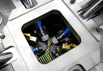
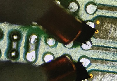
Typical challenges are measurements at chip and board level that require narrow or wide pitch RF probes in GS/SG, GSG as well as GSGS, GSSG and SGS configurations; system calibration at mm-wave frequencies with suppressed higher-order modes; probing of rough, non-planar device pads with different metallization that quickly oxidizes (such as Cu) and plating materials that are difficult to penetrate through, such as ENIG, ENEPIG, organic solderability preservative (OSP).
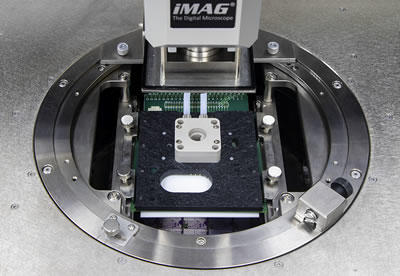
Other challenges include tight integration of the test instrumentation components with the probe system platform; stable, rock-solid system platform; management of large PCB boards, accessibility of the device under test from different sides and angles over long distances; high stability, positioning accuracy and repeatability of the chuck and probe positioners, as well as high magnification optical system with good field of view/resolution ratio, and wide working distance; stable microscope bridge with quick wide-range movement capability and precise final adjustment.
Last but certainly not least is the need for accurate mm-wave system RF calibration suitable for both off-the-shelf alumina and optimized custom-made calibration standards embedded on test coupons.
MPI Solutions
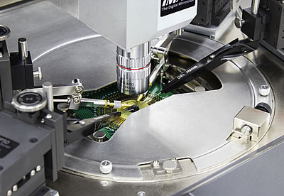
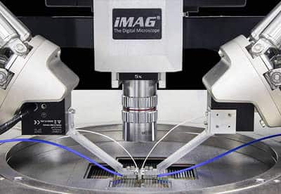
MPI Corporation designed the dedicated 300 mm TS300-PCB Manual Probe System and 600 mm TS600-PCB Manual Probe Systems addressing all the measurement needs of PCB devices at RF and mmW frequency ranges. The rock-solid system platform and features such as the unique platen lift, Probe Hover Control PHC™ , MPI iMAG® digital microscope series, stable microscope bridge with the wide fast movement range, large probe platen, industry-benchmark MicroPositioners together with various options for the vibration isolation table – all these solutions and technologies serve for unmatched quality and repeatability of calibration and measurement results.
Significant productivity improvements can be achieved by an optional motorized microscope stage and SENTIO® - revolutionary multi-touch, single window GUI probe system control software suite.
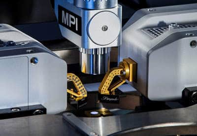
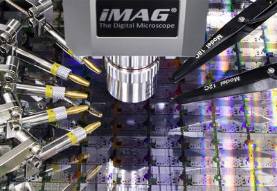
MPI TITAN™ RF Probes provide easy and sure probing of devices with rough and uneven pads, fastest time-to-data and highest measurement throughput especially for multiport system configurations as TITAN™ RF probes can tolerate tips-to-pads planarization errors and often does not require initial probe planarization.
Reliable and repeatable TDR measurements that represent a true device impedance profile that is not affected by the pad oxide resistance can be achieved from the first touchdown, thanks to unique, sharp 3D tips and efficient force deliver mechanism of TITAN™ RF Probes. All these can be achieved on any type of device/trace pad metallization, ENIG, ENEPIG or OSP plating.
Simple measurements at every level of the product integration, chip interface, high-density interfaces (HDI) and PCB with the same tips of probes by the wide variety of the TITAN™ Probe pitch offered from 50㎛ and up to 1250 ㎛ in GS/SG, GSG. GSGSG, GSSG as well as SGS configurations and up to 110 GHz frequency band.
Direct mount of the Dual TITAN™ probes with the TDR remote heads and the solid TDR heads integration on MPI MicroPositioners produce the most accurate TDR results.
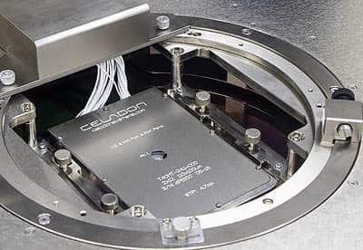
Accurate probe-tip system calibration at mm-wave frequencies with commercially available alumina coplanar calibration standards by the dedicated ceramic AUX chucks that are integrated with the PCB holder.
Trustable over-temperature measurement data by optional thermal chucks up 300 mm size and TITAN™ RF Probes with the temperature range up to +175°C.
System calibration up to four ports with commercially available and custom-made calibration standards, conventional SOLT, MPI proprietary mm-wave optimized TMR/TMRR and metrology-level NIST multiline TRL system calibration by MPI’s RF calibration software QAlibria® that is tightly integrated with NIST StatistiCal software. Simple management of RF probes and standards electrical models with extensive and customer-open QAlibria® probes and standards database.